

TPU7x (Ironwood)
This page describes the architecture and available configurations for TPU7x, the latest TPU available on Google Cloud. TPU7x is the first release within the Ironwood family, Google Cloud's seventh generation TPU. The Ironwood generation is designed for large-scale AI training and inference.
With a 9,216-chip footprint per Pod, TPU7x shares many similarities with TPU v5p. TPU7x provides high performance for large scale dense and MoE models, pre-training, sampling and decode-heavy inference.
To use TPU7x, you can use Google Kubernetes Engine (GKE) or Compute Engine. For more information about using TPUs with GKE, see About TPUs in GKE.
You can also use TPU7x and GKE with All Capacity mode. All Capacity mode is available through an All Capacity mode reservation, which gives you full access to all of your reserved capacity (no hold-backs) and full visibility into the TPU hardware topology, utilization status, and health status. For more information, see All Capacity mode overview.
System architecture
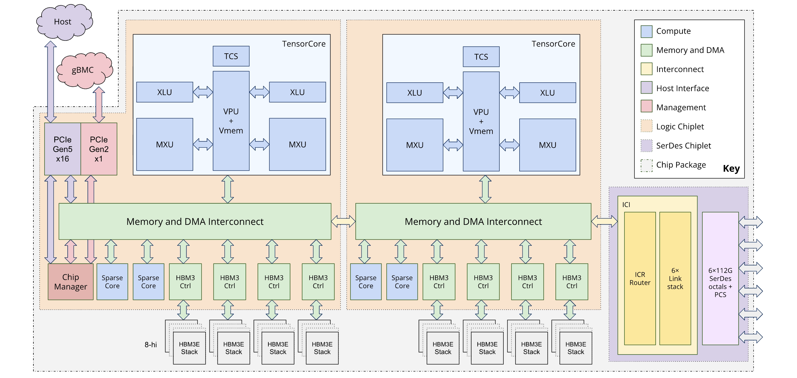
Each TPU7x chip contains two TensorCores and four SparseCores. The following table shows the key specifications and their values for TPU7x compared to prior generations.
| Specification | v5p | v6e (Trillium) | TPU7x (Ironwood) |
|---|---|---|---|
| Number of chips per pod | 8960 | 256 | 9216 |
| Peak compute per chip (BF16) (TFLOPs) | 459 | 918 | 2307 |
| Peak compute per chip (FP8) (TFLOPs) | 459 | 918 | 4614 |
| HBM capacity per chip (GiB) | 95 | 32 | 192 |
| HBM bandwidth per chip (GBps) | 2765 | 1638 | 7380 |
| Number of vCPUs (4-chip VM) | 208 | 180 | 224 |
| RAM (GB) (4-chip VM) | 448 | 720 | 960 |
| Number of TensorCores per chip | 2 | 1 | 2 |
| Number of SparseCores per chip | 4 | 2 | 4 |
| Bidirectional inter-chip interconnect (ICI) bandwidth per chip (GBps) | 1200 | 800 | 1200 |
| Data center network (DCN) bandwidth per chip (Gbps) | 50 | 100 | 100 |
The following diagram illustrates the architecture of Ironwood:
Memory hierarchy
TPU7x features a multi-tiered memory system, and managing data movement between these tiers is crucial for performance:
- High-bandwidth memory (HBM): Each chip is equipped with 192 GB of HBM, with bandwidth of approximately 7.37 TB/s. The large HBM capacity enables large batch sizes, which can improve throughput. However, despite its size, HBM can still be a bottleneck, particularly for memory-bound vector operations or inefficient data access patterns.
- Vector memory (VMEM): VMEM is a smaller, on-chip SRAM (static random-access memory) with significantly higher bandwidth to the Matrix Multiply Unit (MXU) than HBM. This memory acts as a high-speed scratchpad for custom kernels. The size of this buffer is a tunable parameter. Optimizing the buffer size is critical for tuning custom Pallas kernels, as their block sizes are often constrained by the available VMEM.
- Host memory and PCIe: Each set of four TPU chips is connected to a CPU host using a PCIe network. While this connection has much lower bandwidth than HBM, the host's main memory can be used for offloading activations or optimizer states to free up HBM, a technique particularly useful for managing memory pressure in large models.
For more on efficiently managing data movement between the tiers of the TPU7x memory hierarchy, see Ironwood performance optimizations.
Dual-chiplet architecture
The Ironwood programming model lets you access two TPU chiplets instead of a single logical core (also known as MegaCore) architecture used in previous generations (TPU v4 and v5p). This change improves the cost-effectiveness and efficiency of manufacturing the chip. While this represents an architectural shift, the new design ensures that you can reuse existing software models with minimal changes.
Ironwood TPUs are composed of two distinct chiplets, each with its own dedicated memory space. This is a departure from the unified memory space of the MegaCore architecture.
Chiplet composition: Each chiplet is a self-contained unit with one TensorCore, two SparseCores, and 96 GB of high-bandwidth memory (HBM).
High-speed interconnect: The two chiplets are connected by a die-to-die (D2D) interface that is six times faster than a 1D inter-chip interconnect (ICI) link. Inter-chiplet communication is managed using collective operations.
Programming model and framework exposure
The programming model for Ironwood is similar to that of TPU generations earlier than v4, such as TPU v3. The new architecture is exposed in the following ways:
Two devices per chip: Frameworks like JAX expose each Ironwood chip as two separate "devices," one for each chiplet.
Chiplet specification: You can specify which chiplet to use for a computation. JAX adds a fourth dimension to the topology specification to distinguish between chiplets. This design lets you reuse existing software models with minimal changes.
For more information about achieving optimal performance with the dual-chiplet architecture, see Performance recommendations for Ironwood's dual-chiplet architecture
Supported configurations
TPU7x chips have a direct connection to the nearest neighboring chips in 3 dimensions, resulting in a 3D mesh of networking connections. Slices larger than 64 chips are made up of one or more 4x4x4 "cubes" of chips.
TPU7x chips have a 3D torus interconnect topology. This topology allows slices to scale up to 9216 chips. It has bi-directional bandwidth of 200 GBps per axis for communication between chips within a pod.
The following table shows common 3D slice shapes that are supported for TPU7x:
| Topology | TPU chips | Hosts | VMs | Cubes | Scope |
|---|---|---|---|---|---|
| 2x2x1 | 4 | 1 | 1 | 1/16 | Single-host |
| 2x2x2 | 8 | 2 | 2 | 1/8 | Multi-host |
| 2x2x4 | 16 | 4 | 4 | 1/4 | Multi-host |
| 2x4x4 | 32 | 8 | 8 | 1/2 | Multi-host |
| 4x4x4 | 64 | 16 | 16 | 1 | Multi-host |
| 4x4x8 | 128 | 32 | 32 | 2 | Multi-host |
| 4x8x8 | 256 | 64 | 64 | 4 | Multi-host |
| 8x8x8 | 512 | 128 | 128 | 8 | Multi-host |
| 8x8x16 | 1024 | 256 | 256 | 16 | Multi-host |
| 8x16x16 | 2048 | 512 | 512 | 32 | Multi-host |
TPU7x VM
Each TPU7x virtual machine (VM) contains 4 chips. Each VM has access to two NUMA nodes. For more information about NUMA nodes, see Non-uniform memory access on Wikipedia.
All TPU7x slices use full-host, 4-chip VMs. The technical specifications for a TPU7x VM are:
- Number of vCPUs per VM: 224
- RAM per VM: 960 GB
- Number of NUMA nodes per VM: 2
Supported models
A supported model is tuned and validated for TPU7x hardware. You can deploy and run supported models without code changes. Supported models are configured to take advantage of TPU7x features, including the dual-chiplet architecture, high-bandwidth interconnects (ICI), HBM, and mixed-precision compute (such as FP8 and BF16).
Google and the open-source community maintain pre-tuned recipes, configurations, and support for both training and inference workloads on TPU7x.
Training-optimized models
Training-optimized models include pre-configured recipes and hyperparameters tuned for distributed training frameworks. These recipes configure optimal parallelism strategies (including data, tensor, pipeline, and context parallelism) to maximize throughput and scaling efficiency across single-host and multi-slice TPU7x topologies.
To find training recipes, guides, and performance benchmarks for supported models on TPU7x, see the following resources:
- TPU training recipes for TPU7x: The official GitHub repository containing pre-tuned training recipes, precision configurations (FP8 and BF16), step-time benchmarks, and throughput metrics for popular open models on TPU7x.
- MaxText repository: An open-source, high-performance LLM training framework written in JAX and optimized for Cloud TPU.
- Train a model using TPU7x: A guide for provisioning TPU7x resources and deploying training workloads with MaxText.
Inference-optimized models
Inference-optimized models are validated for high-performance serving using
vLLM and the
tpu-inference plugin. These
models are tested for correctness, numerical accuracy, and serving throughput,
leveraging optimized PagedAttention kernels and tensor parallelism on TPU7x.
To find serving recipes and deployment tools for supported models on TPU7x, see the following resources:
- TPU inference recipes for TPU7x: Pre-tuned vLLM serving recipes, configurations, and deployment manifests optimized for TPU7x.
tpu-inferenceGitHub repository: The open-source TPU backend plugin for vLLM, providing hardware-optimized kernels and execution backends for JAX and PyTorch models.- TPU v7x vLLM model support matrix: Nightly automated test results for unit tests, correctness, and benchmark status on TPU7x.
- Run inference on Cloud TPU: A guide for setting up single-host model serving on Cloud TPU.
Hyperdisk
By default, the VM boot disk for TPU7x is Hyperdisk Balanced. You can attach more disks to your TPU VM for additional storage. The following disk types are supported on TPU7x:
- Hyperdisk Balanced
- Hyperdisk ML
For more information about Hyperdisk, see Hyperdisk overview. For more information about storage options for Cloud TPU, see Storage options for Cloud TPU data.
What's next
- Use TPU7x with GKE
- Use TPU7x with All Capacity mode
- Use the Google Cloud ML Diagnostics platform to optimize and diagnose your workloads
- Run a training workload using a recipe optimized for TPU7x
- Run a TPU7x microbenchmark
- Ironwood performance optimizations
- Train large-scale machine learning models on GKE with Multi-Tier Checkpointing